ChipVORX® IP for Ultra Fast Flash Programming
ChipVORX® Accelerator IP enables ultra fast in-system Flash programming

ChipVORX® Flash Accelerator IP library enables FPGA-based ultra fast in-system programming (ISP) of Flash components via standard 1149.1 Test Access Port (JTAG interface). Developed ChipVORX® models are intelligent IPs that reduce the programming time of every kind of Flash memories at full workflow automation. In practice, the ChipVORX® IPs achieve drastic accelerations for bigger FPGA types compared to standard Boundary Scan programming procedures. Whilst typical values for parallel Flash are in the range of 10x - 15x, the factor for serial Flash, where the configuration time becomes really critical, can easily go up to 100x. In many cases, the acceleration is only limited by the Flash internal programming speed. The usage of the IP does neither require expert background knowledge nor special FPGA design tools or programmer.
Download informative booklet about ChipVORX Flash Accelerator (PDF, 2.5MB)
Technology highlights:
- Universal push-button solution: no extra engineering efforts
- Immediately speeds-ups flash programming by 10-15 times
- Up to 100x acceleration can be achieved for Flash memories with serial interface
- Support for all latest Xilinx and Altera FPGAs
- Lattice and Actel FPGAs are supported upon request
- Tightly integrated with Goepel Electronic’ SYSTEM CASCON
- Automated flash program generation (AFPG)
- No FPGA design knowledge or third-party design tools required
- Support of advanced custom IPs for maximally fast Flash ISP on specific target board
Prerequisites:
- Availability of FPGA device that is attached to the target flash IC
- System CASCON 4.5.4 from Goepel electronic with valid maintenance contract
- Valid ChipVORX® license
- Valid license for Flash ISP
Flash Acceleration performance
Flash Accelerator turns hours into minutues... and minutes into seconds
We have thoroughly tested different boards to measure the performance achieved by ChipVORX® Flash Acceleration.
| System / Test type | Traditional ISP | Flash Accelerator | Speed-up |
|---|---|---|---|
| Xilinx development board, Virtex5 (XC5VLX110T), parallel 16-bit NOR Flash (JS28F256), SPI flash (25P32V6P) | |||
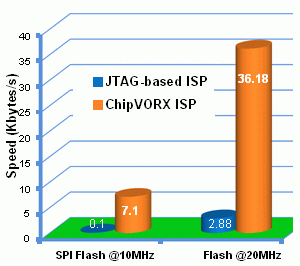
| NOR Program+Verify 1MB @20MHz | 5m 56s | 34s | 10.5 |
| SPI Program 1MB @10MHz | 1h 25m 50s | 1m 12s | 71.5 |
| XESS development board, Spartan3a (XC3S1000), parallel 16-bit NOR Flash (S29AL016) | |||
| Program+Verify 1MB @10MHz | 13m 47s | 1m 16s | 10.9 |
| Blank Check 1MB @10MHz | 4m 18s | 26s | 9.8 |
| Commercial board, Spartan3a (XC3S200A), parallel NAND flash (K9F2G08) | |||
| NAND Flash 32MB Program, 20MHz | 38m 2s | 4m 6s | 9.3 |
| NAND Flash 32MB Verify, 20MHz | 40m 23s | 6m 21s | 6.4 |
| GÖPEL VarioTAP Coach Board, Spartan3a (XC3S50A), parallel NOR flash (S29AL008), SPI flash (VS1011E_S) | |||
| NOR Flash Program+Verify | 1m 35 s | 19 s | 3.8 |
| SPI Flash Program+Verify | 49 s | 3.5 s | 14.0 |
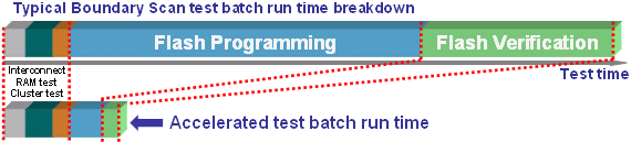
Overall Boundary Scan test flow acceleration
In-system Flash configuration is typically the most time-consuming task in the Boundary Scan test flow. While the time required for other tests (tests for opens and shorts, memory interfaces and logic clusters testing, clock presence detection) is normally measured in seconds, Flash programming and verification can easily take hours, especially in case of large data images and Flashes with serial interface (e.g. SPI). ChipVORX® Flash accelerator is capable to drastically change the typical breakdown of Boundary Scan test time.
Extra performance
Do you need extra performance beyond the existing off-the-shelf ChipVORX® Flash Accelerator IP solution? Contact us to request full custom Flash Accelerator IP to achieve maximal possible Flash programming speed on specific target board. Contact ChipVORX team at chipvorx[at]testonica.com
Integrated and automated solution
Flash programming acceleration just by a single click on "Use Accelerator" checkbox
The ChipVORX® Flash Accelerator technology is fully integrated into Goepel Electronic’ SYSTEM CASCON software platform thus the recognition of connections between Flash target and FPGA as well as generation of flash programming speed is done automatically. Because of the ChipVORX® IP’s independence of the target to be programmed, the Flash type imposes no restrictions. In addition to serial Flash, parallel NOR and NAND Flash incl. bad block handling are supported. As the same system libraries as for a “normal” Boundary Scan programming are used, users may update new Flash models by themselves.
Existing Boundary Scan projects prepared using Goepel's SYSTEM CASCON toolsuite can be accelerated just by a single click on "Use Acceleration" option. Flash Accelerator is fully integrated into CASLAN test language and uses standard CASCON AFPG model for support of the communication protocol with the target Flash component. This means that test engineer has the full control over Flash programming and verification flow.
Supported FPGA devices
ChipVORX® Accelerator supports vast majority of modern FPGA devices
At the moment, the ChipVORX® models for Flash programming are available for all Altera and Xilinx FPGA families, additional ones are under development. The full support is provided for the following families:
- Spartan–3, Spartan–3A, Spartan–3AN, Spartan–3E, Spartan–3A DSP, Spartan–6
- Virtex–4, Virtex–5, Virtex–6
- Arria GX, Arria II GX
- Cyclone, Cyclone II, Cyclone III, Cyclone IV
- Stratix, Stratix II, Stratix III, Stratix IV
The support for Lattice and Actel FPGAs as well as for older Altera and Xilinx devices is also provided upon request.
Technology description
ChipVORX is based on an innovative concept of intelligent embedded instrumentation
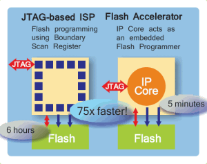
Traditional in-system programming is performed by using on-board JTAG-compliant device that is connected to target Flash component. The access to Flash is organized via standard Boundary Scan shift register (BSR) that allow to control and observe the state of each pin of JTAG device during its operation. However in order to access Flash through JTAG device, external tester needs to perform complete shift cycle of BSR in order to activate appropriate signals on Flash bus. However, the length of BSR chain can reach up to several thousands of separate flipflops for the complex devices. As a result, traditional ISP tools cannot provide high speed of communication with target Flash devices.
Currently, modern complex electronic boards typically include an FPGA device, which is connected to target Flash. In this case, a specialized embeddable Flash Accelerator IP can replace traditional Boundary Scan ISP flow. Instead of using of BSR scan register, Flash accelerator downloads a special pre-compiled instrument IP into the onboard FPGA. The instrument is then used to quickly program or verify data image to the target flash IC. Because ChipVORX IP are stored in a pre-compiled way, no third-party design software or VHDL knowledge is required.
For detailed information about ChipVORX technology please contact us at chipvorx[at]testonica.com
Download informative booklet about ChipVORX Flash Accelerator (PDF, 2.5MB)