ChipVORX® Embedded Virtual Instruments for ISP, Test and Measurement
ChipVORX® intelligent IP cores provide embedded virtual instrumentation framework
![]()
ChipVORX® technology developed by Testonica Lab and Goepel electronic uses available system resources to enable specialized IPs to be embedded into system and act as virtual instruments. The target functionality of ChipVORX® instruments covers wide range of various test, measurement and ISP tasks such like ultra-fast Flash programming, precise clock measurements, high-speed or at-speed test of memory interfaces (incl. DDR2/DDR3 memories) and I/O ports. The ChipVORX® solutions are fully integrated into system CASCON from Goepel electronic.
Flash Accelerator
Flash Accelerator IP enables ultra fast in-system Flash programming via standard JTAG interface

ChipVORX® Flash Accelerator IP library reduces the programming time of every kind of Flash memories at full workflow automation. In practice, the intelligent ChipVORX® IPs achieve drastic acceleration for bigger FPGA types compared to standard Boundary Scan programming procedures. Whilst typical values for parallel Flash are in the range of 10x - 15x, the factor for serial Flash, where the configuration time becomes really critical, can easily go up to 100x. The usage of the IP does neither require expert background knowledge nor special FPGA design tools or programmer.
Download informative booklet about ChipVORX Flash Accelerator (PDF, 2.5MB)
High-speed interconnect test of DDR/2/3 memories
Communication with high-performance memories in Boundary Scan test flow

Special ChipVORX® IP enables the functionality for testing of high-speed memory devices, which cannot be achievable when using pure Boundary Scan access since that DDR2 and DDR3 are not guaranteed to be working at low frequencies. Moreove, static Boundary Scan testing is unable to detect timing inconsistencies in propagated signals (delay or transition faults).
ChipVORX® DDR IP provides high-speed communication with DDR, DDR2 and DDR3 memory interfaces and is perfectly suitable for testing high-speed memory devices.
Precise clock measurements
Use ChipVORX® IP to precisely measure clock frequency via standard JTAG access port
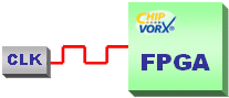
With traditional Boundary Scan tools it is not possible to adequately measure the frequency of clock signal. Pure Boundary Scan technique can only check whether clock signal makes transitions from HIGH to LOW and back, however the period of oscillation will not even be assessed.
ChipVORX® clock IP is a reliable instrument that is capable to accurately measure clock frequency (incl. differential clock) without usage of external equipment such as oscilloscope or frequency counter. The measurement is performed by using on-board FPGA device (to which clock net is attached) and standard Boundary Scan test access port (JTAG). The presicion of measurement depends on target clock frequency and available TCK speed is normally in the range of 0.1MHz – 0.01MHz.
Combining several instruments together
ChipVORX® technology is flexible enough for combining several instruments inside single IP core

With ChipVORX® technology it is possible to effectively unite various test, measurement and ISP functionality inside single multifunctional instrument. This gives a unique opportunity to sequentially perform several test tasks without need to reconfigure FPGA each time. Because the process of reconfiguration of complex FPGA devices can take up to several minutes, a great time saving is achieved.
Contact ChipVORX team at chipvorx[at]testonica.com