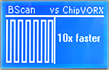
Embedded ChipVORX® IP Enables Ultra Fast Flash Programming

GOEPEL electronic, world-class vendor of JTAG/Boundary Scan solutions announces the first product based on its new ChipVORX® technology at the International Test Conference (ITC'2010) in Austin, TX, USA. The new ChipVORX® based embedded instrumentation solution, developed in cooperation with the Tallinn/Estonia based Company Testonica Lab within the frame of the GATE alliance, is structured modularly as a set of ChipVORX® models and intelligent IPs. They enable the ultra fast in-system programming of every kind of Flash components at full workflow automation.
"The FPGA based accelerated procedure, developed by Testonica, enables the extremely fast Flash programming. Additionally, it is fully automatable, which fits perfectly to our revolutionary new ChipVORX technology to control chip embedded instrumentations", says Thomas Wenzel, GOEPEL electronic’s managing director of the Boundary Scan Division. "By the complete integration into our SYSTEM CASCON software platform, users can now fast and effectively program massive Flash images with the existing tool suite. Furthermore, the tremendous advantages in in-system programming can be implemented even stronger in particular in the production process, and will replace cost intensive stand-alone solutions."
Dr. Artur Jutman, Testonica Lab's Director adds: "Our key challenge was to deliver customers a technology with a great added value and absolutely no penalty in form of personnel training and extra time spent for project configuration. Now, engineers can considerably speed-up their in-system programming tasks just by enabling a license. The technology will be demanded in applications involving large flash memories especially flash ICs equipped with a serial interface."
Due to the complete integration of the ChipVORX® IP the recognition of the structural connections between Flash target and FPGA is done as automatically as the succeeding script file generation. The programming is based on a standardised IEEE1149.1 TAP (Test Access Port), and can be executed on each run time station without further options. Thereby, Gang applications are supported.
Due to the ChipVORX® IP’s independence of the target to be programmed, the Flash type imposes no restrictions. In addition to serial Flash, parallel NOR and NAND Flash incl. bad block handling are supported. As the same system libraries as for a "normal" Boundary Scan programming are used, users may update new Flash models by themselves.
In practice, the ChipVORX® IPs achieve drastic accelerations for bigger FPGA types compared to standard Boundary Scan programming procedures. Whilst typical values for parallel Flash are in the range of 10x - 15x, the factor for serial Flash, where the configuration time becomes really critical, can easily go up to 100x. In many cases, the acceleration is only limited by the Flash internal programming speed.
At the moment, the ChipVORX® models for Flash programming are available for all Altera and Xilinx FPGA families, additional ones are under development. The usage of the IP does neither require expert background knowledge nor special FPGA tools or programmer.
